External switching power supplies are a critical component in modern electronics, providing safe, efficient, and reliable power for consumer, industrial, and medical devices. As devices become more compact and performance-driven, understanding the internal structure and design considerations of these power supplies is essential for engineers, product designers, and technical enthusiasts.
This article provides a comprehensive, in-depth overview of external switching power supplies, covering functional blocks, design principles, reliability considerations, testing, and future trends.
1. Introduction
Switching power supplies have transformed electronic systems by replacing traditional linear power supplies with high-efficiency, compact alternatives. External switching power supply is particularly favored because it allows isolation of high-voltage circuitry, simplifies system design, and ensures user safety.
Key advantages of external switching power supplies include:
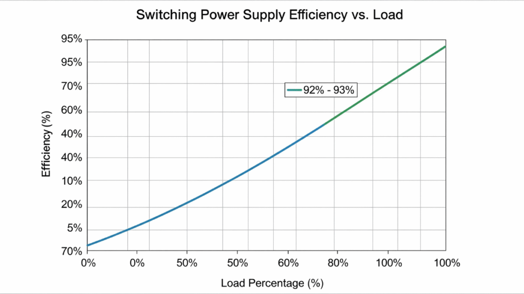
- High efficiency: Typically 80–95%, reducing energy loss and heat generation.
- Compact size: High-frequency operation enables smaller transformers and passive components.
- Safety: Isolation barriers protect users and sensitive components.
- Modularity: Easy replacement or upgrade without redesigning the host device.
Applications
External switching power supplies are widely used across industries:
- Consumer electronics: Laptops, routers, gaming consoles, LED lighting.
- Industrial systems: PLCs, sensors, motor controllers.
- Medical devices: Monitors, diagnostic tools, and smart beds.
- Automotive electronics: EV chargers, infotainment systems.
By understanding their internal design, engineers can improve efficiency, reduce EMI, and extend device lifespan.
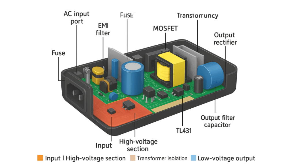
2. Internal Functional Blocks
A typical external switching power supply consists of several interconnected functional stages:
- AC Input and Protection – ensures safe mains connection.
- EMI Filtering – suppresses electromagnetic interference.
- Primary Rectification and DC Bus – converts AC to high-voltage DC.
- High-Voltage Switching Stage – MOSFETs controlled by PWM convert DC to high-frequency AC.
- High-Frequency Transformer – provides voltage conversion and isolation.
- Secondary Rectification and Output Filtering – converts AC to a regulated DC output.
- Feedback and Regulation Loop – maintains output voltage stability.
Each stage has unique design considerations affecting efficiency, reliability, and compliance.
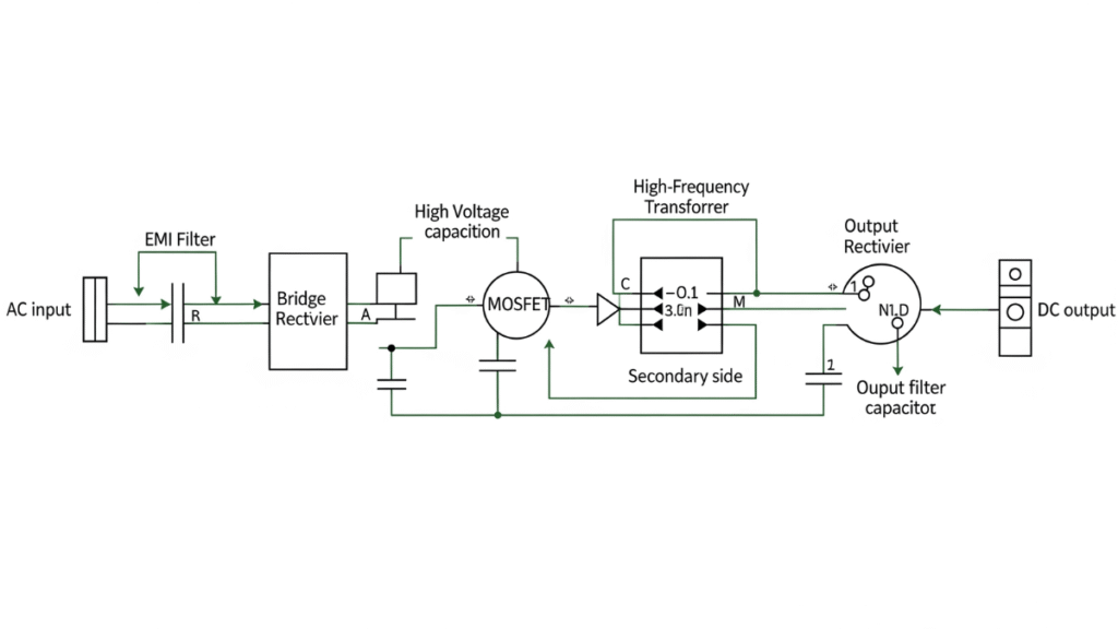
3. AC Input and Protection Stage
The AC input stage safeguards the power supply and connected devices. Key components include:
- Fuse: Provides overcurrent protection. Selection depends on rated current, type (fast-blow or time-delay), and operating environment.
- NTC Thermistor: Limits inrush current at power-on.
- MOV (Metal Oxide Varistor): Protects against voltage surges and transients.
- Gas Discharge Tube (GDT): Optional for high-voltage surge protection.
Example Calculation – MOV Clamping Voltage:
For 230V AC mains:
V_peak = V_RMS * sqrt(2) ≈ 230 * 1.414 ≈ 325 V
Choose MOV with clamping voltage slightly above peak, e.g., 350–400 V, to protect downstream components.
Inrush Current Control:
I_inrush = V_peak / R_NTC
This design minimizes fuse stress and prolongs the life of rectifiers and DC bus capacitors.
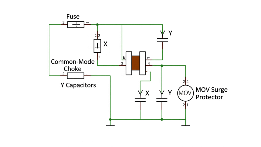
4. EMI Filtering Stage
EMI filtering ensures compliance with standards like CISPR 22, FCC Part 15, and regional regulations. Key design points include:
- Common-mode choke: Reduces common-mode noise; core material selection affects frequency response.
- X-Capacitors: Connected line-to-line; Class X2 for safety.
- Y-Capacitors: Line-to-ground; Class Y1/Y2 for insulation.
Testing & Optimization:
- Conducted EMI spectra measured before and after filtering.
- Adjust capacitor values and choke design to minimize emission peaks.
- PCB layout critical: short high-current loops and separate high-frequency paths.
5. Primary Rectification and DC Bus
AC mains is converted to DC via a full-bridge rectifier, followed by a high-voltage capacitor forming the DC bus.
- Diode Selection: Must withstand reverse voltage and surge currents.
- Capacitor Rating: Ripple current and voltage rating determine longevity.
DC Bus Voltage Example:
For 230V AC mains:
V_DC = V_AC_peak - V_diode_drop ≈ 325 V - 1.4 V ≈ 323.6 V
Ripple Voltage:
V_ripple = I_load / (f * C_bus)
Ripple affects MOSFET switching stability and secondary output quality.
6. High-Voltage Switching Stage
High-voltage MOSFETs operate in PWM switching mode. Design considerations:
- Rds(on), Vds, Gate Charge (Qg), Avalanche Energy
- Gate Drive Waveform: Proper shaping reduces EMI and switching losses.
- PWM Control: Voltage-mode vs current-mode, each with pros and cons.
- Soft-start Mechanism: Reduces inrush and component stress.
Waveform analysis shows transitions, ringing, and overshoot mitigation.
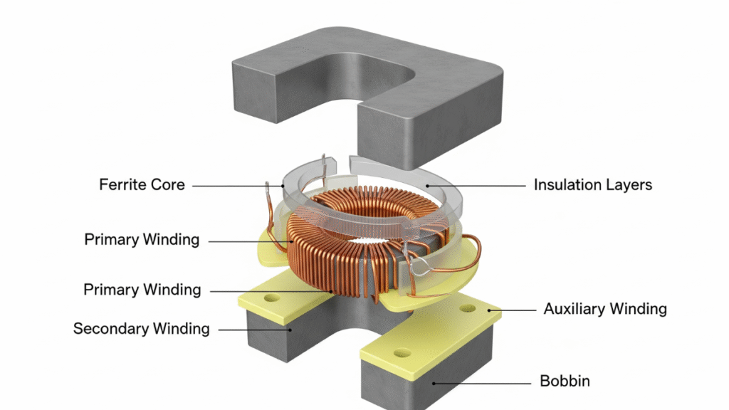
7. High-Frequency Transformer Design
Compact ferrite transformers provide voltage conversion and isolation at high frequency:
- Core Types: EE, ER, PQ; selection impacts leakage inductance and flux density.
- Material Selection: Determines saturation flux, thermal stability, and efficiency.
- Turns Ratio: Based on DC bus and output voltage requirements.
- Insulation & Safety: Creepage and clearance distances must meet IEC/UL standards.
Layered winding reduces leakage and improves EMI performance.
8. Secondary Rectification and Output Filtering
The transformer secondary is rectified and filtered to produce regulated DC:
- Schottky Diodes: Low forward drop, fast recovery.
- Synchronous Rectification: Reduces conduction losses at higher currents.
- LC Filters: Smooth ripple and stabilize voltage.
Output Ripple Calculation:
V_ripple = I_load * ESR + I_load / (f * C_out)
Ensures connected devices receive clean, stable power.
9. Feedback and Regulation Loop
Maintaining output voltage stability involves:
- TL431 Precision Reference
- Optocoupler: Provides primary-secondary isolation.
- Compensation Network: Ensures loop stability; Bode plot analysis confirms phase margin.
Temperature effects and CTR degradation are critical for long-term stability.
10. PCB Layout and Thermal Management
PCB layout affects safety, EMI, and thermal performance:
- Primary/Secondary Separation: Maintain proper creepage and clearance.
- High di/dt Loop Minimization: Reduces EMI.
- Thermal Management: Copper pours and thermal vias for heat dissipation.
- Component Placement: EMI filters near AC input; high-current paths short and wide.
11. Reliability and Failure Analysis
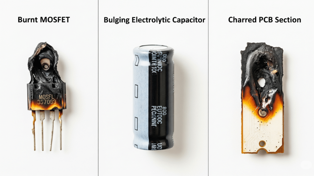
Common failures:
- Electrolytic capacitor bulging or leakage
- MOSFET breakdown due to overvoltage or thermal stress
- Transformer insulation degradation
Accelerated Life Testing:
- Thermal cycling
- High-temperature operation
- Humidity exposure
Analyzing failure cases informs design improvements.
12. Testing and Quality Assurance
Comprehensive testing ensures performance and compliance:
- Electrical Tests: Load regulation, efficiency, transient response
- Safety Tests: Dielectric withstand, insulation resistance, leakage current
- EMC Compliance: Pre-compliance testing before certification
- Burn-in Procedures: Detect early failures
These steps guarantee reliability across applications.
13. Compliance with International Standards
External switching power supplies must comply with:
- IEC 62368-1, UL, CCC, PSE
- Energy Efficiency: DOE Level VI, EU ErP Lot 6
- Standby Power Limits
Certification involves documentation, testing, and factory audits.
14. Applications Across Industries
- Consumer Electronics: Laptops, LED lighting, IoT devices
- Industrial Equipment: PLCs, sensors, robotic controllers
- Medical Devices: Monitors, smart beds, diagnostic tools
- Automotive Electronics: EV charging systems, infotainment
Tailored designs meet different voltage, current, and environmental requirements
15. Future Trends
- GaN-Based Switching Devices: Higher efficiency, smaller size
- USB Power Delivery & Multi-Voltage Designs
- Wireless Charging Integration
- AI-Assisted Power Management: Predictive maintenance and energy optimization
These trends define the next generation of external switching power supplies.
16. Conclusion
External switching power supplies are critical enablers of modern electronics. Careful design, rigorous testing, and adherence to standards ensure:
- Safety and reliability
- High efficiency and EMI compliance
- Long-term durability
Continuous innovation in materials, switching technology, and intelligent management ensures these power supplies remain at the forefront of electronic design.